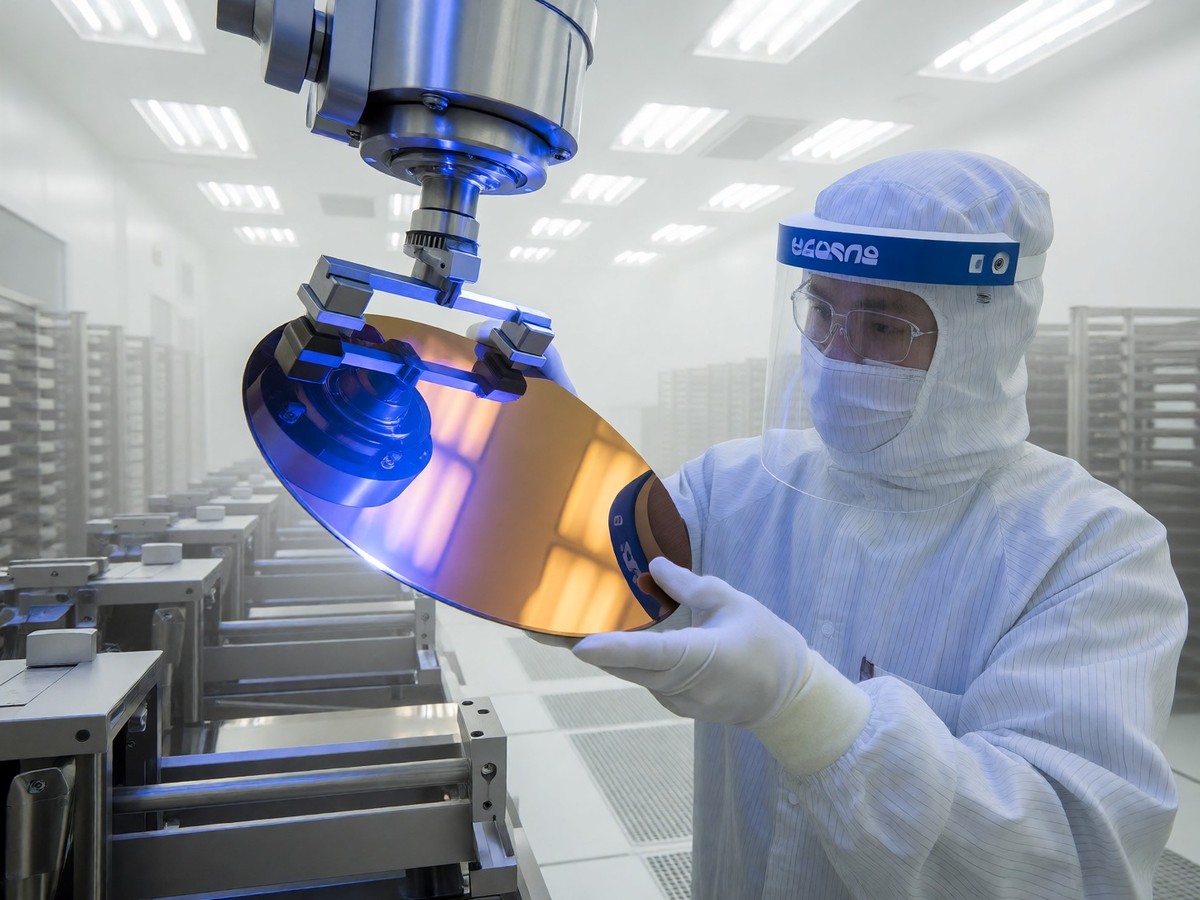
Nvidia faces a manufacturing squeeze because TSMC’s CoWoS-L packaging capacity remains the primary constraint for Blackwell Ultra production. While TSMC aims to reach 130,000 CoWoS wafers per month by late 2026, the company remains fully booked with lead times between 52 and 78 weeks. Nvidia holds roughly 60% of this capacity, claiming 510,000 CoWoS wafers specifically for CoWoS-L. This concentration leaves Broadcom with 15% and AMD with 11%.
The shortage stems from physical assembly needs rather than wafer fabrication. TSMC can etch more GPU dies than it can package. A GPU requires both a CoWoS slot and HBM stacks. Solving one alone moves nothing. Extra HBM with no packaging capacity results in inventory. Extra packaging capacity with no HBM results in idle line time.
Thermal management issues also plague the Blackwell architecture. A mismatch in the coefficient of thermal expansion among the GPU chiplets, the LSI bridges, the RDL interposer, and the motherboard substrate causes warping and system failure. Nvidia had to redesign the top metal layers and bumps of the GPU silicon to improve yields. This redesign forces a requalification process with TSMC before mass production begins.
| Component | 2026 Status | Lead Time |
|---|---|---|
| CoWoS-L | Fully booked | 52 – 78 weeks |
| HBM3e | Sold out | N/A |
| HBM4 | Ramping | N/A |
| N3 Logic | Tight | 52 – 78 weeks |
Memory and hyperscaler demand
High Bandwidth Memory (HBM) availability creates a second bottleneck. HBM3e is sold out for 2026, with prices increasing by double digits year-over-year. SK Hynix supplies approximately 62% of Nvidia’s HBM4 and roughly two-thirds of its HBM3e. This supply concentration forces Nvidia to rely on a single primary partner to meet its roadmap.
Microsoft is attempting to reduce its dependence on Nvidia by building custom silicon. Microsoft is in discussions with TSMC to secure manufacturing capacity for over 300,000 Maia 300 chips for 2027 delivery. This follows the January launch of the Maia 200. Microsoft aims to produce gigawatts of capacity through these custom chips.
Large cloud providers also consume the remaining supply through massive forward orders. Microsoft, Google, Meta, and Amazon placed multi-billion-dollar orders for Blackwell GPUs in 2025. These orders consume most of the available allocation through 2026 and 2027. These commitments crowd out mid-market and enterprise customers who previously bought through standard channels.
I find the reliance on a single packaging technology for the entire roadmap risky. If TSMC cannot resolve the warping issues in CoWoS-L, the entire Blackwell ramp stalls.
Blackwell Ultra specifications
Blackwell Ultra targets the AI factory market using a dual-reticle design. This design connects two reticle-sized dies using the NVIDIA High-Bandwidth Interface, which provides 10 TB/s of bandwidth. The chip utilizes TSMC 4NP manufacturing and contains 208 billion transistors.
The memory subsystem in Blackwell Ultra provides 288 GB of HBM3e per GPU. This capacity represents a 3.6x increase over the H100 and a 50% increase over the original Blackwell. The total bandwidth reaches 8 TB/s per GPU, which is a 2.4x improvement over the H100’s 3.35 TB/s.
| Feature | Blackwell Ultra Spec |
|---|---|
| Transistor Count | 208B |
| Memory Capacity | 288 GB HBM3e |
| Memory Bandwidth | 8 TB/s |
| Tensor Cores | 640 (5th Gen) |
| NVFP4 Compute | 15 PetaFLOPS |
| TDP | 1,400W |
The architecture includes 160 Streaming Multiprocessors organized into eight Graphics Processing Clusters. Each SM contains four fifth-generation Tensor Cores. These cores use the second-generation Transformer Engine to handle NVFP4 precision. This format reduces the memory footprint by 1.8x compared to FP8.
The Blackwell Ultra also doubles the throughput for key instructions in the attention layer. This change allows for 2x faster attention-layer compute compared to previous Blackwell models. This modification targets reasoning models that use large context windows.
The competitive landscape
AMD and custom silicon designs challenge Nvidia’s market position. AMD’s MI325X delivers competitive results against Nvidia’s H100 for certain inference workloads. AMD’s chips deliver 40% more tokens per dollar on LLM inference workloads compared to Nvidia.
Hyperscalers are moving toward self-sufficiency to lower costs. Microsoft’s Maia 200 offers 30% better performance per dollar than the latest generation hardware in its current fleet. Google uses its own TPUs, and Amazon utilizes its own Trainium and Inferentia chips. These custom solutions reduce the high-margin sales available to Nvidia from its largest customers.
The software ecosystem remains Nvidia’s main defense. CUDA provides the programming model for GPU-accelerated computing and has a two-decade head start. Every major deep learning framework like PyTorch and TensorFlow uses CUDA as a native backend. Switching to AMD’s ROCm requires migrating every application, library, and operational workflow.
Can Nvidia maintain its valuation if custom silicon replaces its primary customers?
The market currently views the Blackwell supply issues as a temporary manufacturing hurdle. However, the combination of TSMC packaging limits and the aggressive custom silicon programs at Microsoft and Google creates a difficult environment for Nvidia to sustain its growth rates. The company must manage the transition to CoWoS-L without letting its leading-edge customers migrate to in-house alternatives.
Leave a Reply